INDEX
1. Flash Controller
(1). Flash Controller
(2). Purpose of Use
2. NVMCTRL ( Non-Volatile Memory Controller)
(1). About NVMCTRL
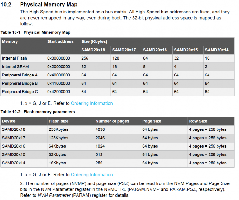
– Physical Memory Map
– NVMCTRL Features
(2). NVMCTRL Command function
– Erase
– Read/Write
– Lock bit
– Security bit
(3). NVMCTRL HandsOn
3. EEFC (Enhanced Embedded Flash Controller)
(1). About EEFC
– Physical Memory Map
– Memory Regions
– NVMCTRL Features
(2). EEFC Command Function
– Read Operations
– Write
– Erase commands
– Lock Bit
– GPNVM BIt
– Security Bit
– unique Identifier Area
(3). EEFC HandsOn
(1). Flash Controller
– Flash Controller는 MCU에 내장된 Flash에 직접 접근하여 제어 할 수 있는 인터페이스이다.
– 특정 Flash Address에 Access, Read, Write, Lock 등 가능하다.
(2). Purpose of use
일반적으로 MCU에 Download(ISP, SWD, JTAG) Interface를 통해 Internal Flash에 firmware나 Data를 programming 한다.
Flash controller는 MCU에 내장되어 있는 Function으로 아래와 같은 개발에 필요한 기능이다.
- 별도의 Bootloader 개발이 필요한 경우
- DownLoad Interface를 사용하지 않고 flash에 programming 해야 하는 경우
- Internal Flash를 다른 용도로 사용해야 하는 경우
32bit ARM Core가 적용된 Microchip MCU에는 NVM Controller와 EEFC라는 이름으로 Flash Controller가
내장 되어 있다.
Microchip ARM Cortex-M0+가 적용된 SAMD,L,C,R 시리즈는 NVMCTRL을 통해 Flash 제어가 가능하다.
Microchip ARM Cortex-M4, M7이 적용된 SAM4, SAMG, SAME,S,V Device들은 EEFC를 통해 Flash 제어를 할 수 있다.
1. NVMCTRL(Non-Volatile Memory Controller)
* NVMCTRL은 32Bit Cortex-M0+가 적용된 SAMD, L, C 시리즈의 내장 Memory Controller이다.
(1). About NVMCTRL
– Physical Memory Map
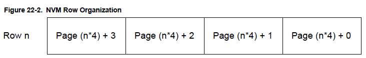
Cortex-M0+ Core의 SAM D, L, C, R 시리즈는 아래와 같이 Memory Map으로 하나의 Page는 64 byte로 구성되어 있으며,
1 row는 4 page(256 byte) 로 구성 되어 있다.
Atmel Cortex-M0+는 Pin count, Flash size 라인업이 구분되며, 14 – 128 pin, 8K – 256K Size에 따라 나뉜다.
– Memory Regions
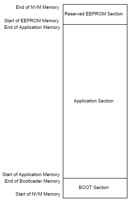
SAMD시리즈의 Memory Region은 BOOT, Application, EEPROM 3가지 영역으로 나누어져 있다. Main Array는 row와 page로 구성되어 있다.
Nvm_get_parameters() 함수를 이용하여 NVM 메모리 공간의 Page size 및 총 page 수와 같은 장치 별 매개 변수를 사용 할 수 있다. (Memory Region은 Device마다 다름.)
NVM PAGE의 Number 및 Address는 아래 방정식을 이용해 구할 수 있다.
PageNum = (RowNum X 4) + PagePosInRow(page position in Row)
PageAddr = PageNum * PageSize
– NVMCTRL Structure and Spec.
Features
- 32-bit AHB interface for reads and writes
- 32-bit APB interface for commands and control
- Read While Write EEPROM emulation area
- All NVM sections are memory mapped to the AHB, including calibration and system configuration
- Programmable wait states for read optimization
- 16 regions can be individually protected or unprotected
- Additional protection for boot loader
- Supports device protection through a security bit
- Interface to Power Manager for power-down of Flash blocks in sleep modes
- Can optionally wake up on exit from sleep or on first access
- Direct-mapped cache
(2). NVMCTRL Command Function
– Erase
Write는 Page 단위로, Erase는 row 단위로만 처리 가능하다. 따라서 row의 한 page만 수정하는 경우,
row의 나머지 page를 buffer에 저장한 후 row 전체를 지운다.
수정한 page와 buffer에 저장된 나머지 page를 합친 후 쓰게 된다. Page에 Write하기 전에 Erase는 필수이다.
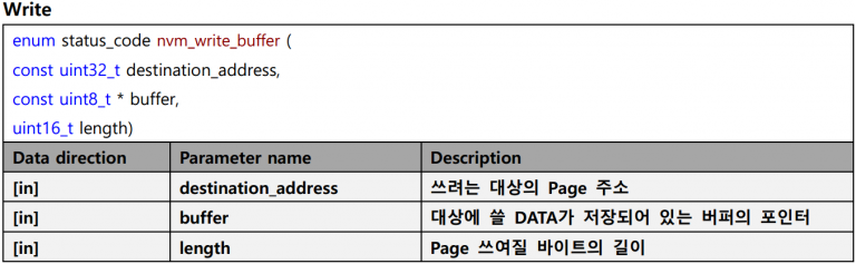
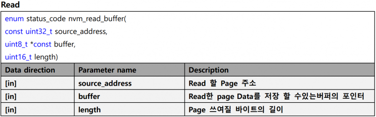
– Read/Write
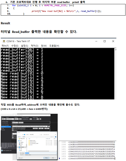
NVM 메모리 Read는 직접 주소 지정을 사용하거나 nvm_read_buffer()함수를 호출하여 수행 한다.
NVM 메모리에 쓰기는 nvm_write_buffer () 함수에 의해 수행할 수 있다.
NVM 컨트롤러가 수동 페이지 쓰기 모드로 구성된 경우, 수동 페이지 프로그램 명령을 실행 해야 한다.
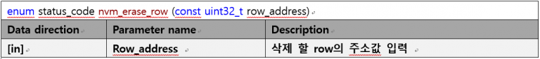
Page 업데이트 시 먼저 NVM 메모리 row을 nvm_erase_row() 함수를 통해 지우고 Writing 한다.
삭제되지 않은 페이지에 기록하면 NVM 메모리 공간에 손상된 데이터가 저장된다.
– Region Lock bits
NVM 메모리의 주요 블록은 개별적 주소 지정이 가능한 여러 Page로 나뉜다.
이 페이지는 동일한 16개 영역으로 그룹화 되며, 각 영역은 NVM_COMMAND_LOCK_REGION command를
nvm_execute_commmand() 함수에 전달하여 사용하거나, row에 직접 Lock bit를 쓰는 방식으로 잠글 수 있다.
* Reserve EEPROM 영역은 Lock 비트와 command의 영향을 받지 않는다. *
– Security bits
Security bit가 설정되면, 사용자 row는 Read나 Wirte를 할 수 없다.
Security bit는 NVM_COMMAND_SET_SECURITY_BIT를 nvm_execute_command() 함수에 전달하여 설정하거나,
사용자가 잠긴 영역에 접근 시도를 하면 설정된다. Security Bit는 chip erase를 수행하면 지워진다.
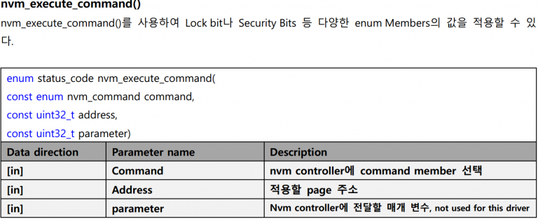
이밖에도 Command Function과 Define된 많은 member를 제공하고 있다.
NVM Application Note – 7. API Overview를 참고.
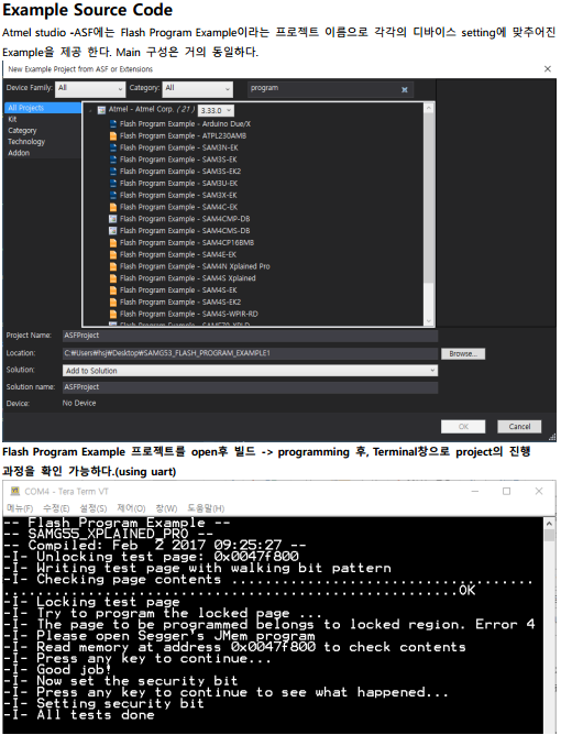
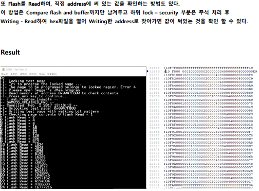
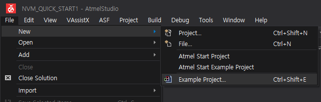
Example Source Code
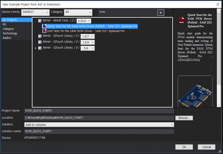
Atmel studio – ASF(Atmel Software Framework)에는 SAMD – NVM 관련 Example 프로젝트를 제공 한다.
Quick start for the SAM NVM Driver(Polled) 예제를 실행한다.


2. EEFC (Enhanced Embedded Flash Controller)
– EEFC는 Cortex-M4, M7코어 MCU에 적용된 내장 Memory Controller이다.
(1). About EEFC
– Physical Memory Map
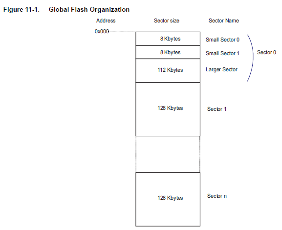
Microchip 32bit 고성능 라인업인 Cortex-M4, M7는 Cortex-M0+와는 다른 메모리 구조를 가지고 있다.
Flash는 Internal bus와 직접 연결 되어 있으며, 다음과 같이 구성 되어 있다.
- 하나의 Memory Plane은 code와 동일한 크기의 여러 Page로 구성
- Unique한 chip identifier를 포함하는 별도로 분리된 2×512 byte 메모리 영역
- User signature를 위한 별도로 분리된 512 byte 메모리 영역
- 최적화 된 Code Read에 사용 가능한 두 개의 128 or 64bit Read buffer
- 최적화 된 Data Read에 사용 가능한 두 개의 128 or 64bit Read buffer
- Page programming을 관리하는 하나의 Write buffer. (size는 page 크기와 같음)
- 여러 page의 Write/Erase 작업을 보호하기 위해 사용되는 여러 개의 잠금 비트(Lock Region)
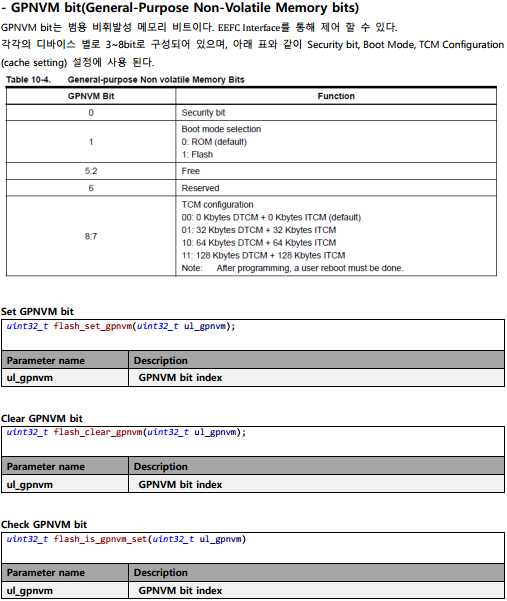
- Non-Volatile Memory bits라고 하며, EEFC Interface를 통해 설정 할 수 있는 비트(GPNVM bits)
– Memory Regions
메모리 Sector는 디바이스별로 size 차이가 있다. 위 그림은 Cortex-m4/SAMG55 기준의 Memory Regions이다.
Sector0는 8Kbyte 2개, sector와 112Kbyte의 1개 총 3개의 sector로 나누어져 있다.
그 외 나머지는 128Kbyte로 된 하나의 Sector로 구성 되어 있다.
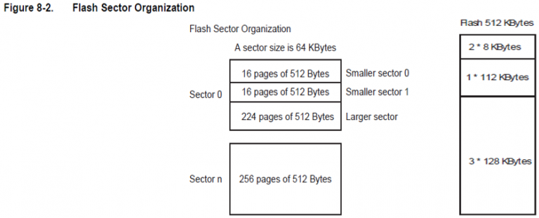
Page단위는 512bytes이며, SAMG55 기준 하나의 Sector는 256page로 구성되어 있다. (Datasheet 참고)
Cortex – M4, M7의 Internal Flash는 모두 주소 0x400000에 Mapping되어 있다.
– EEFC Features
- Increases Performance in Thumb-2 Mode with 128-bit or 64-bit-wide Memory Interface
- Code Loop Optimization
- 64 ~ 128 Lock Bits, Each Protecting a Lock Region
- 3 ~ 8 General-purpose GPNVM Bits
- One-by-one Lock Bit Programming
- Commands Protected by a Keyword
- Erase the Entire Flash
- Erase by Plane
- Erase by Sector
- Erase by Page
- Provides Unique Identifier
- Provides 512-byte User Signature Area
- Supports Erasing before Programming
- Locking and Unlocking Operations
- Supports Read of the Calibration Bits
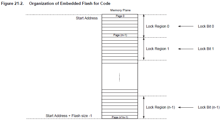
Lock bit Region은 영역은 각 디바이스 별로 차이가 있다.(디바이스별 Datashteet 참조)
영역의 Range는 page 단위로 User가 설정 할 수 있다. Page 주소에 대한 계산식은 아래와 같다.
(Start Address + Flash size – 1)
(2). EEFC Command Function
EEFC Functions에 대한 function descriptor
http://asf.atmel.com/docs/latest/samg/html/group__sam__drivers__efc__group.html
– Read Operations
Optimize된 컨트롤러는 Flash Read를 관리한다. 프로세서가 128bit or 64bit Memory Interface를 통해
Thumb-2 mode로 실행 될 때 성능이 향상된다.
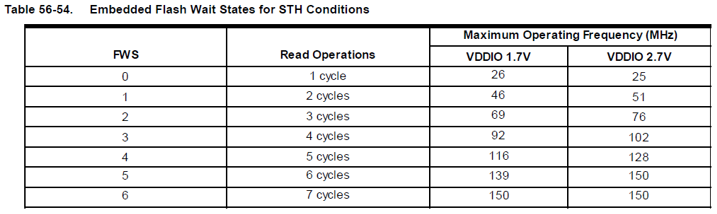
Read는 EEFC_FMR(FWS Field)에 VDD전압과 Clock에 따라 wait stats값을 적절히 넣어 주어 수행 해야 한다.
높은 클럭으로 동작할수록 wait States 수는 커진다. (하단 그림 참조)
기본적으로 Flash Read Access는 128 bit wide interface를 통해 수행 된다. 성능보다 소비 전류가 중요한 경우,
User는 64bit wide memory Interface(EEFC_FMR)를 선택하면 된다.
EEFC Read는 따로 function을 사용하지 않고, pointer로 직접 주소 지정하여 Read가 가능하다.
– Write
EEFC의 여러 가지 command를 사용하여 플래시에 writing할 수 있다. Page에 word를 programming 하려면 우선 page Erase를 해야 한다.
Command로 plane 또는 page 단위로 Erase할 수 있다. Write가 완료 된 후, 여러가지 상황의 write나 Erase를 방지하기 위해 lock을 걸수 있다.
EEFC_FCR에 Programming command를보내기 전에 플래시에 writing할 Data를 내부 latch buffer에 기록해야 한다.
Writing 순서는 아래와 같다.
- 프로그래밍 할 Data를 Latch buffer에 먼저 쓴다.
- EEFC_FCR에 Command 입력(EEFC_FSR.FRDY가 자동으로 Clear)
- 프로그래밍이 완료되면 자동으로 EEFC_FSR.FRDY 자동으로 Toggle 되며, EEFC_RMR. FRDY 활성화 되면, EEFC의 Interrupt가 활성화 된다.
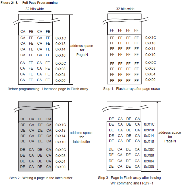
(1). Full Page Programming
- Page의 모든 비트를 erase 한다. .
- Latch buffer에 먼저 Writing한다.
- Write page 명령을 실행하면 latch buffer에 Writing했던 Data가 Flash에 쓰여진다.
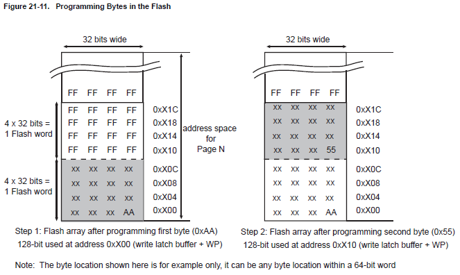
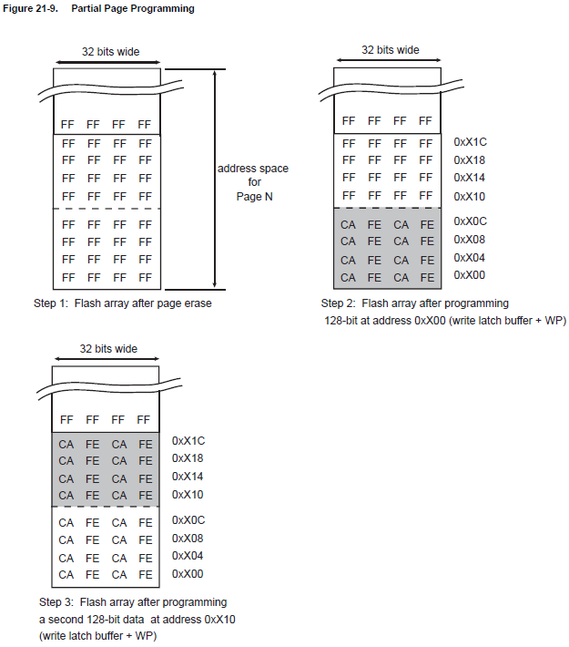
(2). Partial Page Programming
EEFC는 programming할 128bit의 word를 자동으로 감지한다.
- Page의 모든 비트를 erase 한다. .
- 0xX00 번지에 128bit를 프로그래밍 한 후 Flash Array.
- 0xX10 번지에 두번째 128bit Data를 프로그래밍 한 후 Flash Array.
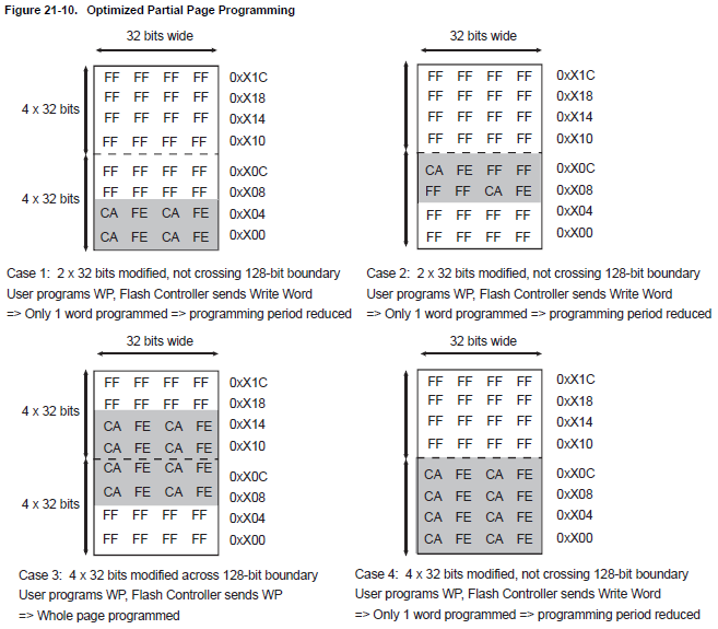
(3). Optimized Partial Page Programming
(4).Programming Bytes in the Flash